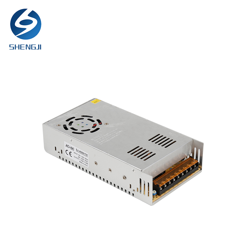
How to Inspect the Appearance of Switching Power Supply
Appearance inspection is mainly to analyze and inspect the appearance defects of switching power supply. The purpose of visual inspection is to record the physical dimensions, materials, design, structure and markings of PCB, electronic parts and solder joints, confirm the defects such as the appearance of damage, and detect the pollution. These problems are errors caused by process manufacturing or application and evidence of overloads and operating errors, and these information are likely to be related to failures.
Appearance inspection is usually used visual inspection, or use 1.5 to 10 times magnifying glass or optical microscope. One of the functions of the visual inspection is to verify the consistency of the PCB, electronic parts and solder joints of the process failure with the standards and specifications; the second function of the visual inspection is to find the problem that may cause the failure. For example, if there are cracks in the shell of the power adapter or charger after being assembled for a period of time, it may be that the compatibility of the two raw material resins of PC/ABS has not been handled well, and it is easy to crack. If there are foreign objects between the outer leads, the foreign objects may cause a short circuit between the leads. Mechanical damage on the PCB surface may cause the PCB trace to break and cause an open circuit.
Since the failure analysis of the switching power supply may be destructive analysis work such as slicing and de-encapsulation, the object of the appearance inspection no longer exists, so detailed records should be made during the appearance inspection, and it is best to take some pictures. As a preliminary inspection, you may lose valuable information if you arbitrarily handle the target before checking the appearance. As part of the visual inspection procedure, firstly, all information marks should be recorded, that is, the names, models, specifications, batches, production dates and other information of PCB manufacturers and electronic parts manufacturers should be recorded in detail. Secondly, special attention should be paid to the inspection of the following aspects:
1. Mechanical damage: cracks, scratches and defects from the pins, roots and sealing seams of the electronic parts; mechanical damage marks on the solder joints and the PCB surface.
2. Device sealing defects: from the joints of the pins of electronic components and glass, ceramics and plastics, as well as the adhesion parts and sealing seams of the roots.
3. Electronic components pin coating defects: uneven coating, bubbles, pinholes and rust spots on the surface of electronic components.
4. Pollution or adhesions on the PCB surface: mainly from the PCB processing process.
5. Thermal damage or electrical damage of the device.
6. PCB delamination and bursting, etc
7. The abnormality of the processing layer of PCB surface.
8. Whether the solder joints are remelted, cracked, or inveracious welded.
When designing the reliability of the switching power supply, it is necessary to put forward clear control requirements for the production, storage, and transportation processes in the process documents. For suspicious parts, further inspections must be performed with measuring instruments that can obtain information and data. All important information is photographed and recorded with microscope and video equipment.


